
High voltage Half-Bridge with Current Feedback using L6390
- Rajkumar Sharma
- 2.717 Views
- medium
- Tested
- SKU: EL102549
- Quote Now
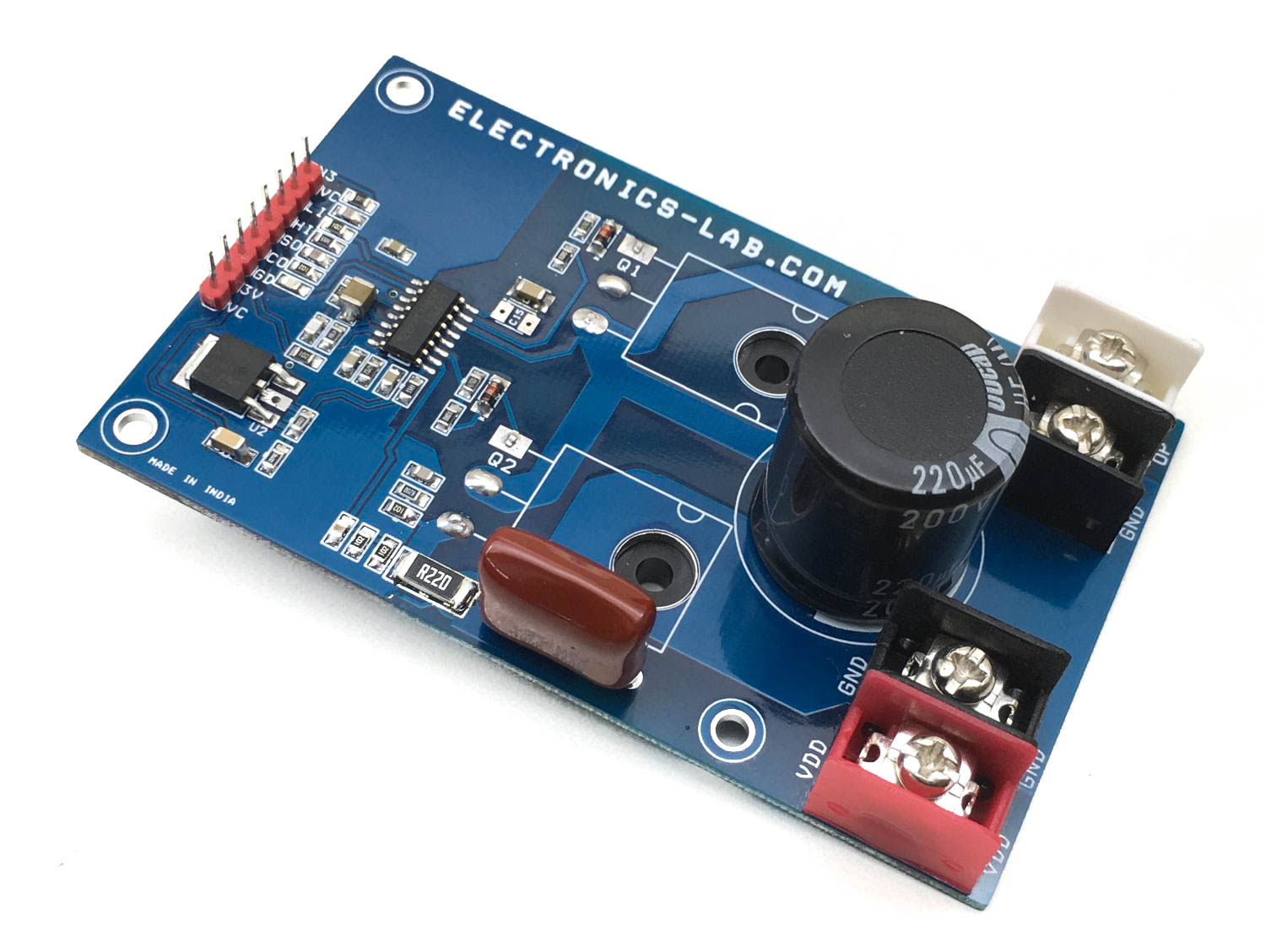
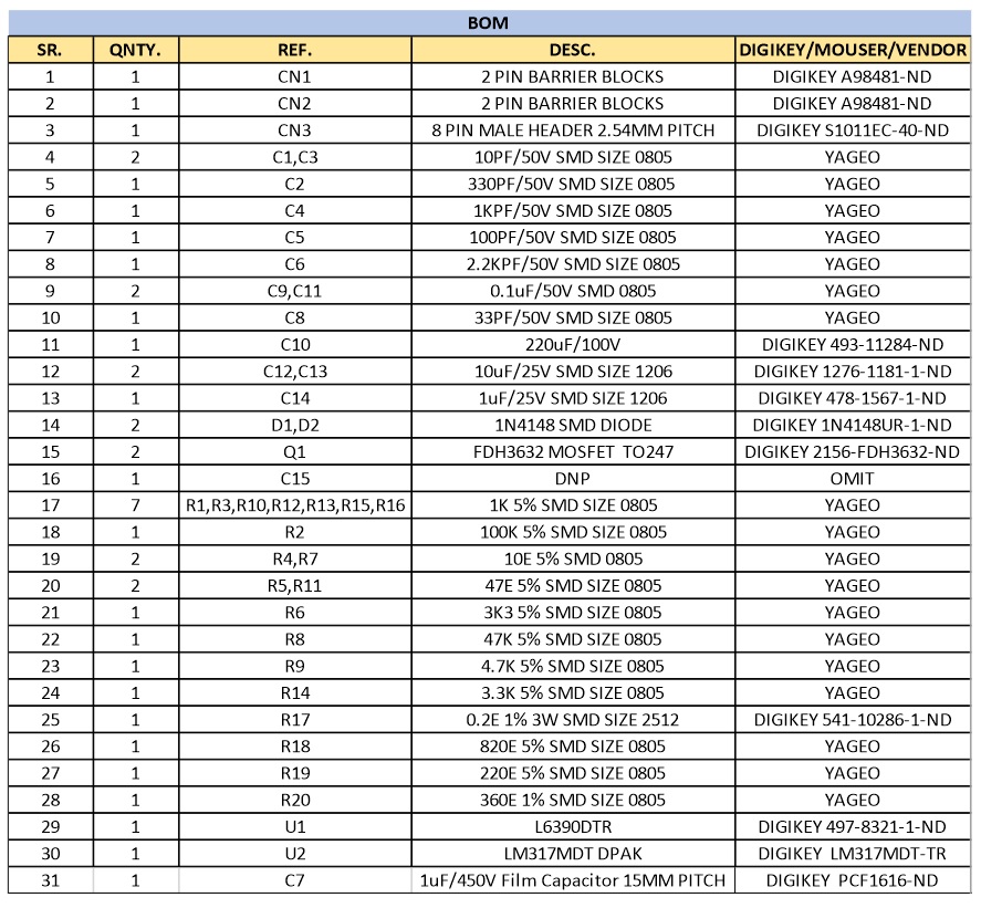
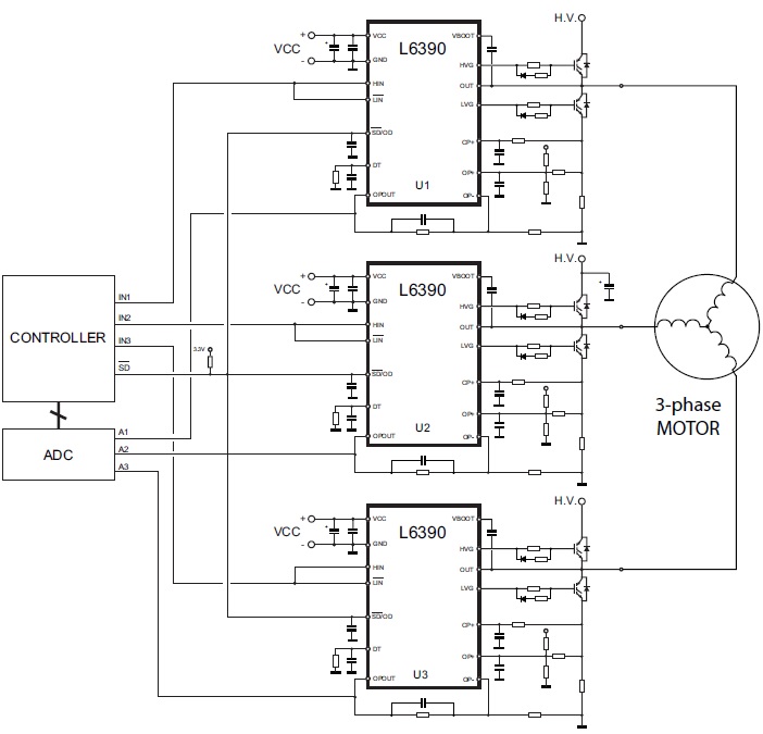
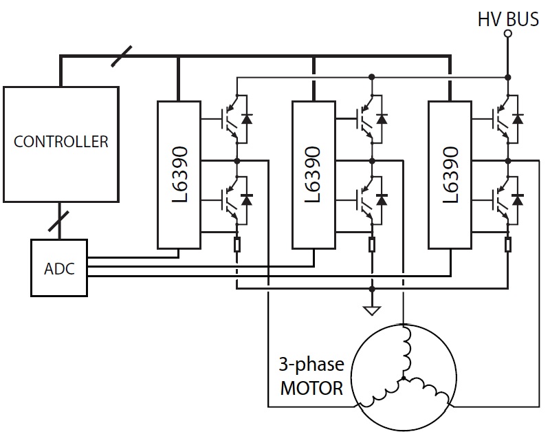
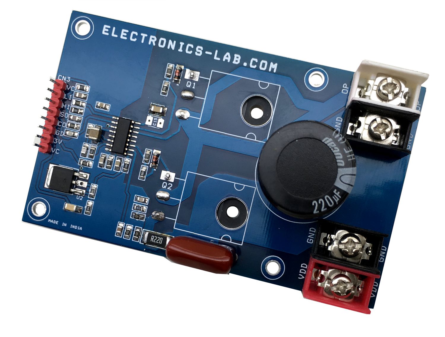
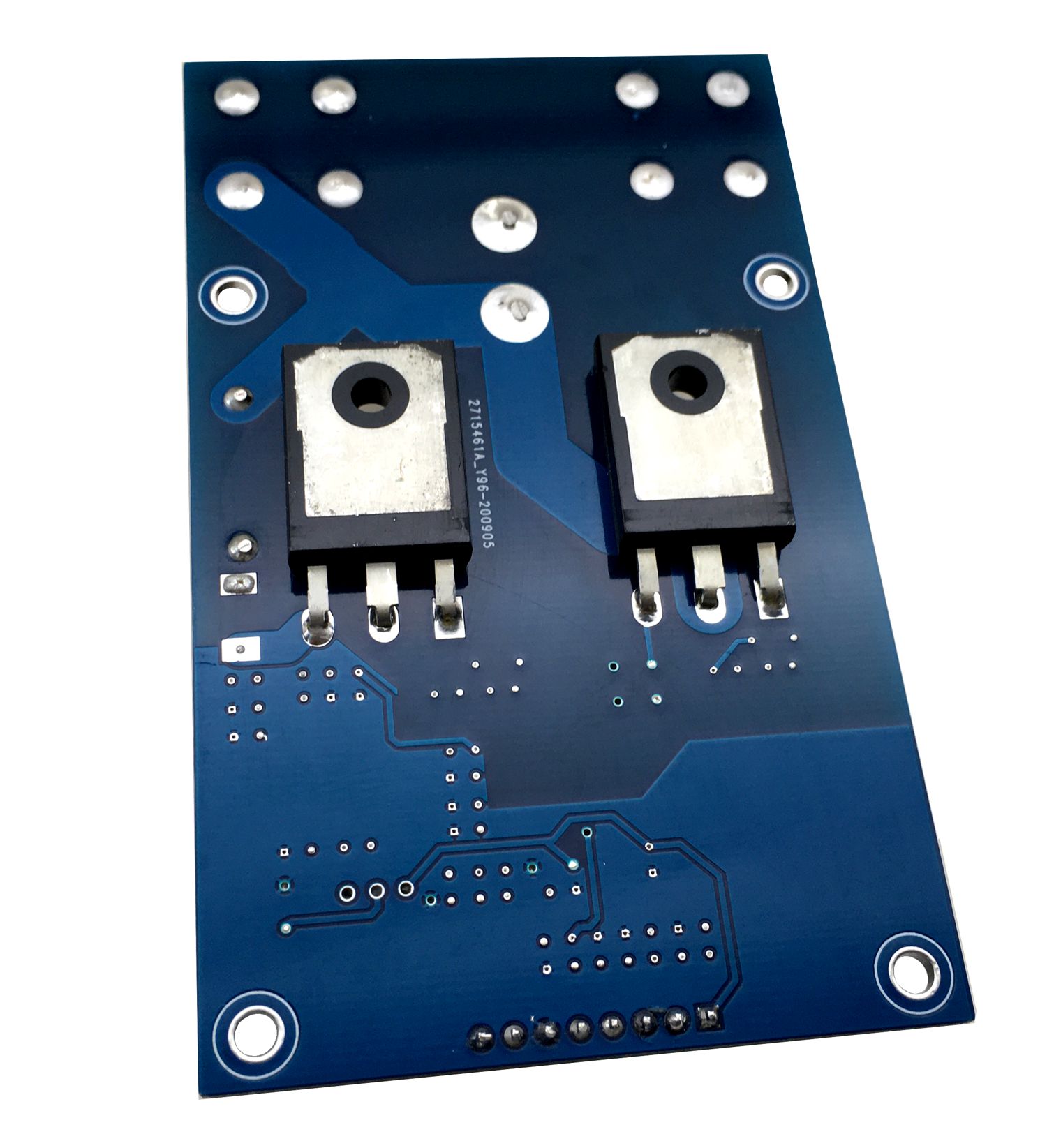
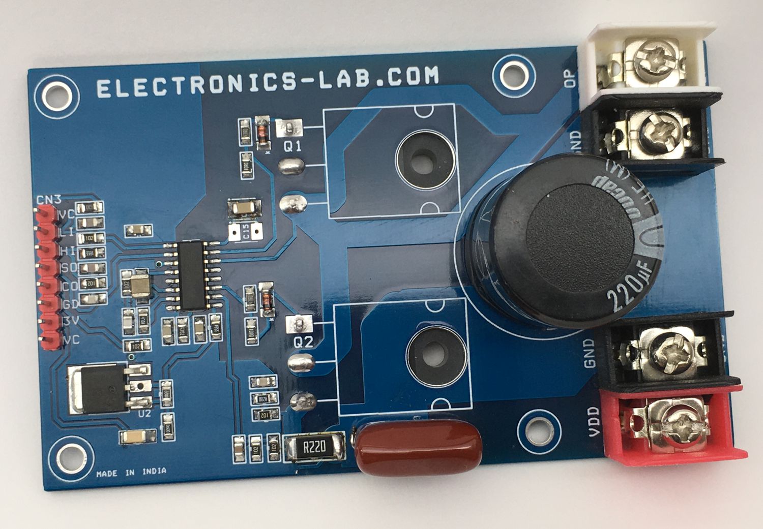
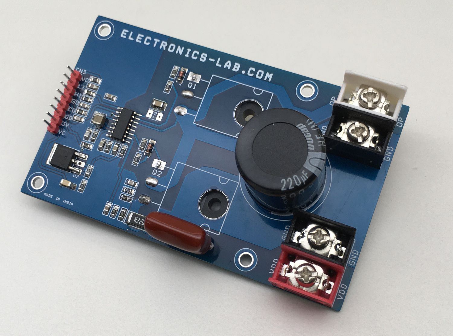
The project presented here is a versatile high voltage Half-Bridge with current feedback. The board is built using L6390 IC from ST Semiconductor. It is suitable for DC-DC converters, EHT drivers, induction heater drivers, battery chargers, LED drivers, DC motor speed controller and field-oriented control (FOC) motor driving application etc. The user can make a FOC Brushless motor driver with 3 of these units, Bidirectional Brushed DC motor can be controlled with 2 units. FDH3632 MOSFETs rated at 100V DC and 80A Current drive the output. Other High voltage and high current MOSFET can be used as per voltage and current requirements.
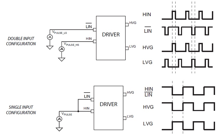
WeI have tested this board with 2A load and input frequency 10-80Khz. This project provides several more functions such as current feedback output, smart shutdown, fault shutdown etc. The board has two logic inputs, HIN and LIN, to separately control the high side and low side outputs, HVG and LVG. HIN is in phase with HVG, while LIN is out of phase with LVG. The signal inversion on the low side input allows control of the half-bridge output with only one control input signal. This board can work with double logic inputs or single input configuration. (See figure below for input configuration). Operating Load power supply 24V – 90V DC and logic supply 12-15V DC. U2 Regulator provides 3.3V DC output to drive Op-Amp circuitry and pull-ups. The board supports input signals 3.3V or 5V. Use large a size heatsink on MOSFETs for heat dissipation.
Features
- Logic Power Supply VCC 12-15V DC
- Load Power Supply VDD 24V-90V DC
- Load 2 Amps (Change R17 Lower resistance and higher wattage for higher current Load)
- Current Feedback Output 2.250V without Load + (0.5V/1Amp)
- Inputs: HIN, 2.LIN, 3. Shutdown
- Outputs: 1. Current Feedback 2. Fault Output
- Input Signal HIN/LIN Frequency 10Khz – 80Khz Logic Level 3.3V/5V DC
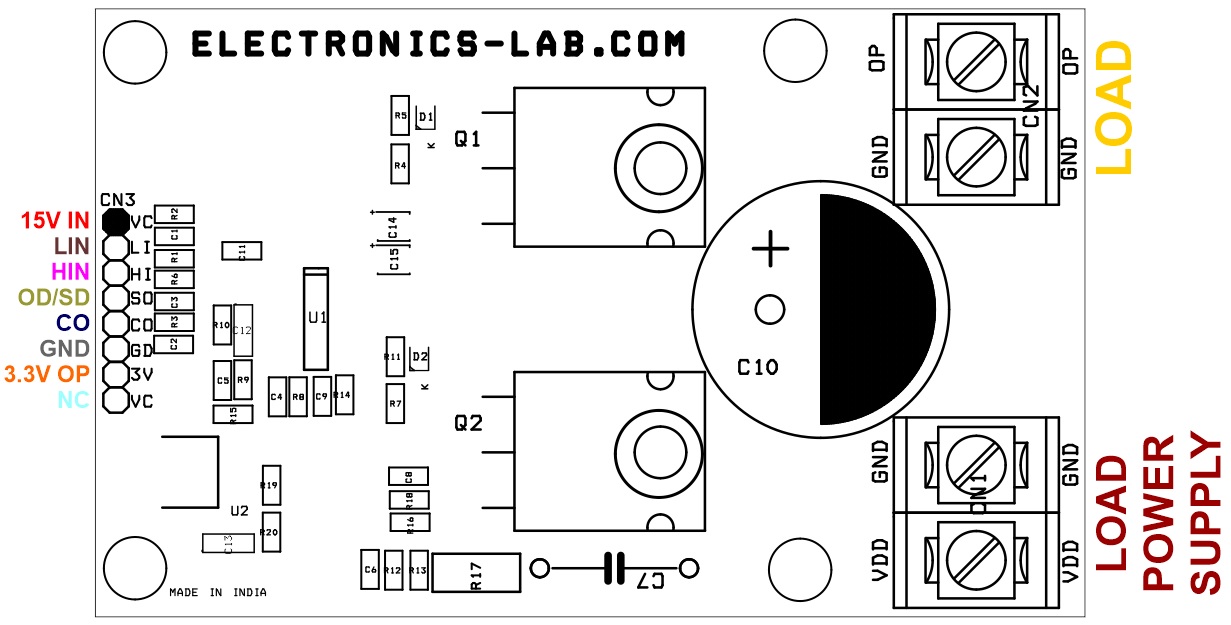
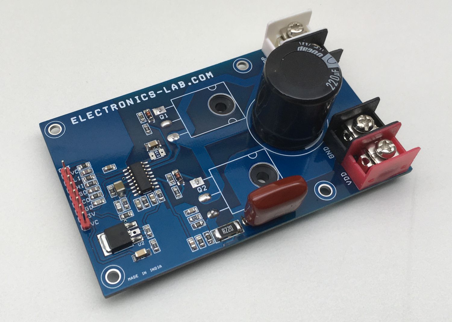
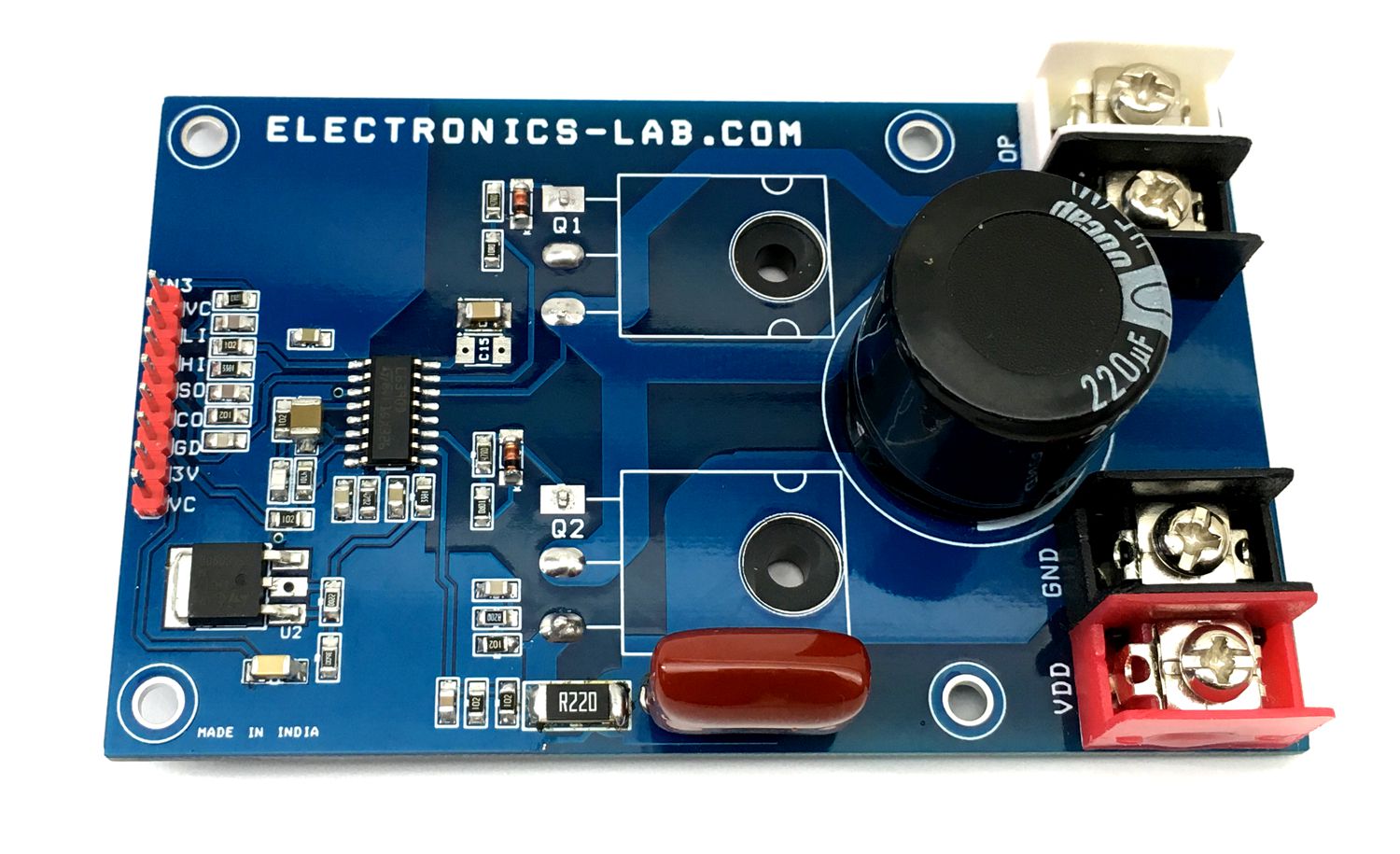
- PCB Dimensions 98.90 x 60.33 mm
Inputs (Logic Inputs 3.3V/5V)
- HIN logic input: 85 kΩ (typ.) pull-down, R6 External pull-down Resistor.
- LIN logic input: 720 kΩ (typ.) pull-up connected to an internal 5 V regulator through a diode, R2 100K External Pull up Resistor
- SD logic input: 375 kΩ (typ.) pull-down, this pin required high logic input to enable the outputs. This pin goes low when fault condition occurs.
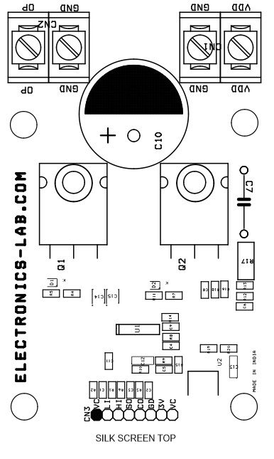
Input Connections CN3
- Pin 1 : VCC 12V – 15 V DC Input Logic Supply /1Amp
- Pin 2 : LIN Signal In
- Pin 3 : HIN Signal In
- Pin 4 : Enable In Pull High/Shutdown Out
- Pin 5 : Current Feed Back Voltage Output
- Pin 6 : GND
- Pin 7 : 3.3V Output Max Load 100mA
- Pin 8 : NC ( Not Connected)
Testing the board
- Apply 12-15V DC to logic supply CN3 VC and GND)
- Apply Load Supply 24 to 30V DC 3Amps to CN1
- Connect the 10 Ohms Resistor at CN2 as load between output and GND
- Tie (Shot)HIN/LIN pin and apply 20Khz Square wave Signal 3.3V/50V DC
- Power on Both Power supply
- Connect the S0 Pin to 3.3V/5V Power source with 10K Series resistor
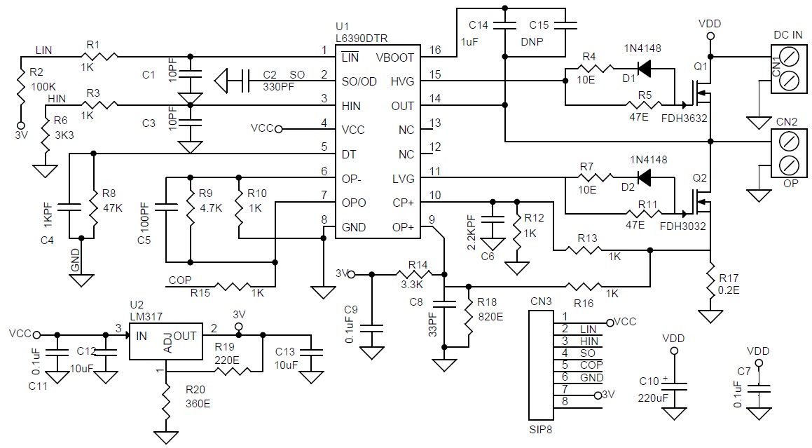
L6390 High voltage high/ low-side driver
The L6390 is a high voltage half-bridge gate driver. This device can be used in all applications where high voltage shifted control is necessary. The devices have a driver current capability best suited for home appliance motor driving ratings, and they are also equipped with patented internal circuitry which replaces the external bootstrap diode. This feature is achieved by means of a high voltage DMOS synchronously driven with the low side gate driver. The L6390 is a half-bridge driver with several functions such as externally adjustable deadtime, interlocking, smart shutdown (patented), fault comparator and a dedicated high-performance op-amp for advanced current sensing. The outputs can be driven by two dedicated logic signals or, alternatively, only one logic signal by connecting the two inputs together. Device outputs can sink and source 430 mA and 290 mA respectively. Prevention from cross conduction is ensured by interlocking and programmable deadtime functions.
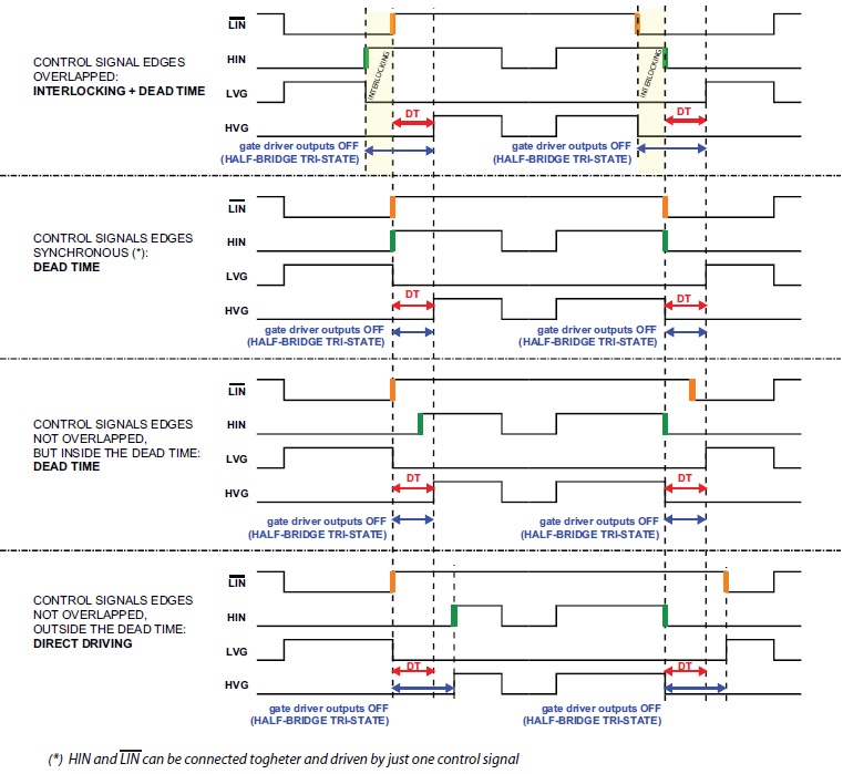
Dead Time: R8 provided to set the Dead time. The dead time can be set to a wide range of values from hundreds of nanoseconds to a few microseconds. In order to avoid any possible cross-conduction between the power MOSFETs/IGBTs of the half-bridge, the L6390 provides both the dead time and the interlocking functions. The interlocking function is a logic operation which sets both the outputs to low level when the inputs are simultaneously active (HIN to high level and LIN to low level). The dead time function is a safety time introduced by the device between the falling edge transition of one driver output and the rising edge of the other output. If the rising edge set externally by the user occurs before the end of this dead time, it is ignored and results delayed until the end of the dead time. The dead time can be adjusted externally through the value of the DT resistor R8 connected between pin 5 and GND. A capacitor C4 1 KPF ceramic capacitor in parallel with this resistor is provided for noise immunity. and interlocking function management are described.
Smart Shut-Down: The L6390 integrates a comparator for fault sensing purposes. The comparator has an internal reference voltage Vref on its inverting input (see L6390 datasheet), while the noninverting input is available on pin 10. The comparator input is connected to an external shunt resistor R17 in order to implement a simple over-current detection function. The output signal of the comparator is fed to an integrated MOSFET with the open drain available on pin 2, shared with the SD input. When the comparator triggers, the device is set in shutdown state and both its outputs are set to low level leading the half bridge in tri-state. In common over-current protection architectures, the comparator output is usually connected to the SD input and an RC network is connected to this SD/OD line in order to provide a mono-stable circuit, which implements a protection time that follows the fault condition. Unlike common fault detection systems, the L6390 smart shutdown architecture allows to immediately turn-off the output gate driver in case of fault, by minimizing the propagation delay between the fault detection event and the actual outputs switch-off. In fact, the time delay between the fault and the outputs turn-off is no more dependent on the RC value of the external network connected to the pin. In the smart shutdown circuitry, the fault signal has a preferential path which directly switches off the outputs after the comparator triggering. At the same time the internal logic turns on the open drain output and holds it on until the SD voltage goes below the SD logic input lower threshold. The smart SD system provides the possibility to increase the time constant of the external RC network (that is the disable time after the fault event) without increasing the delay time of the protection. Any external signal provided to the SD pin is not latched and can be used as control signal in order to perform, for instance, PWM chopping through this pin. In fact, when a PWM signal is applied to the SD input and the logic inputs of the gate driver are stable, the outputs switch from the low level to the state defined by the logic inputs and vice-versa.
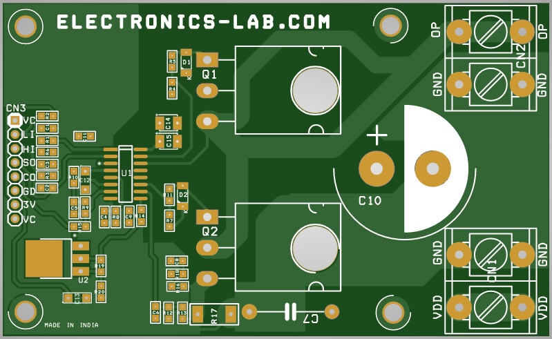
Schematic
Parts List
Connections
3-Phase Configuration
Timing Diagrams
Input Configuration
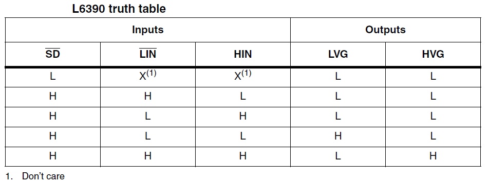
Truth Table
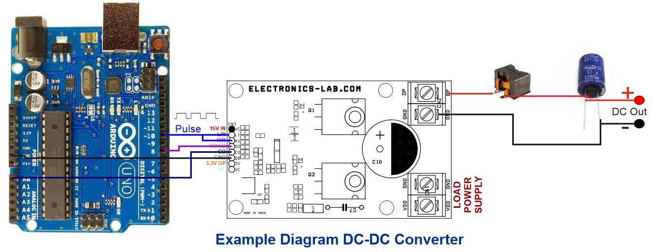
DC-DC Converter Example
Gerber View
Photos
Video
L6390 Datasheet
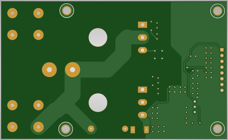
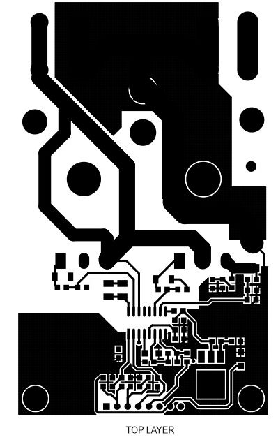
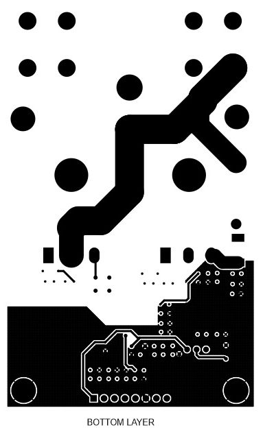
PCB
.png)


")
")