Balanced Audio to Unbalance Converter
- Rajkumar Sharma
- 20.694 Views
- moderate
- Tested
- SKU: EL62833
- Quote Now
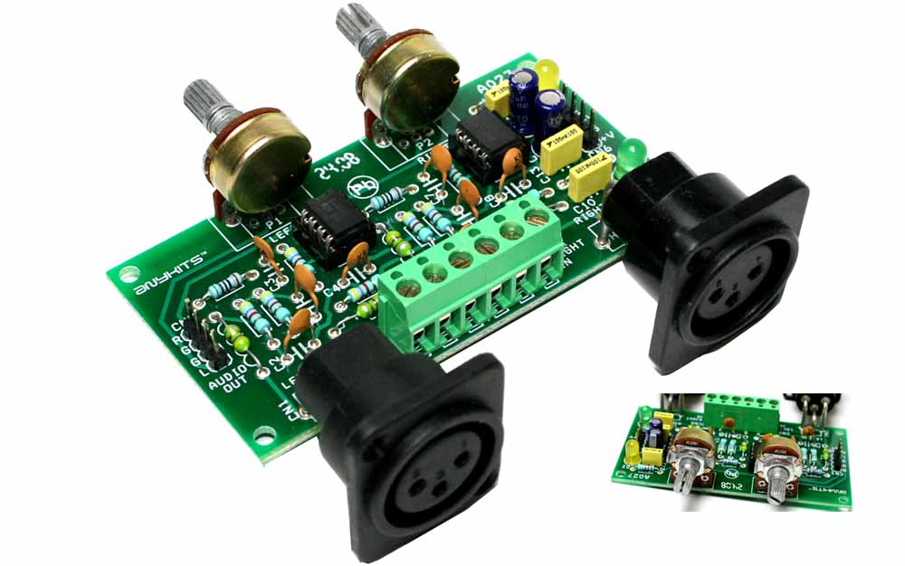
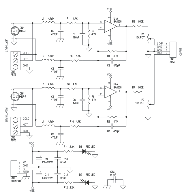
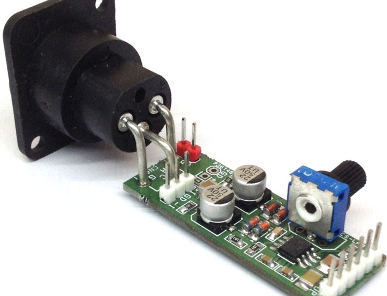
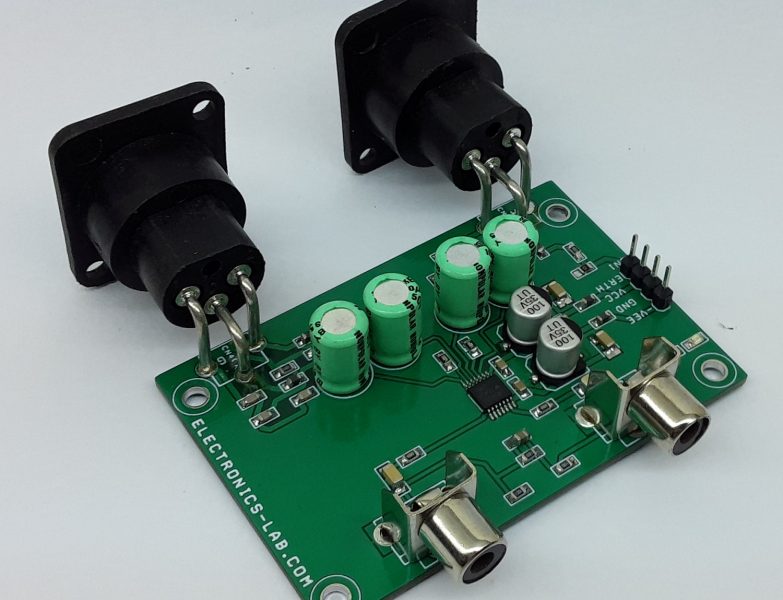
High quality low noise Balance to unbalanced converter designed around op-amps. The project can be used as balance to unbalance converter with on board audio level adjust potentiometer. The project work with +/-15V dual DC supply and draw approximately 100 mA. Board has separate screw terminal for Euro balance audio signal input connector. Dual LED provided for power indication. Input has RFI filter (Inductor)
Specifications
- XLR connectors for stereo audio input
- Screw terminal for Euro Balance audio input standard
- Onboard dual power LED
- Supply dual 15 VDC @ 100 mA
- Header connector for supply input
- Header connector for audio output
- Potentiometer for audio level adjust


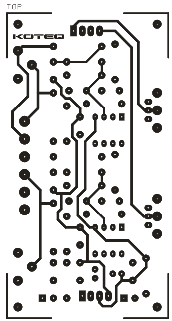
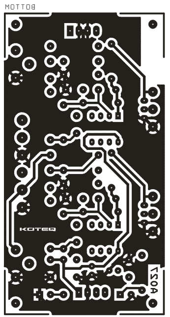
.png)


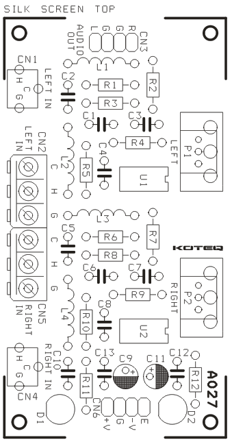
this pcb top side not made as mirror.
Are you going to print it on a transparency?
Hi,
Great and simple solution for this problem. Thank you!
I made another schematic largely based on yours to make a solution for 1 XLR balanced input to 2x unbalanced mono on TRS jack.
I need this setup since the device, I use, expects a stereo signal unbalanced on TRS jack.
So, I split the input signal from the XLR in 2 and make use of the second amp in the BA4560 IC. The 2 outputs which are identical go then to the T and R of the Jack with a common S.
On my PCB I made 2 XLR inputs with 2 TRS (mono) outputs.
But something went wrong:
On XLR input 1 I have the output T that works fine, the other output R is distorted and a bit quieter.
On XLR input 2 I have the output R that works fine, but the T is distorted (exactly the same as the output R in input 1).
The potentiometers work fine on all outputs.
I made the pcb almost entirely with SMD components in order to minimise pcb surface.
I cannot publish the schematics here … any suggestion what could be wrong? Might there be a component broken?
Do you mind opening a new topic in the community, so you can also share your files and we will try to help there? https://www.electronics-lab.com/community/