Simple Soft Latch Switch using Push-Button
- Emmanuel Odunlade
- https://twitter.com/emmaodunlade
- emmaodunlade@gmail.com
- 21.060 Views
- moderate
- Tested
Latching Toggle switches are one of the most popular kinds of switches, from their use by kids in basic electricity classes to their use in prototypes and more advanced products, they provide a familiar and reliable way to close or open a circuit. This makes them the go to switch for designers in most applications but while they may be perfect for switching your device on/off in a low volume project, their price does not make them worthy for use in large scale projects as they can be expensive (usually over a dollar depending on the current rating you require), comparing the fact that you could buy a microcontroller and other components for that price. Due to these costs, designers, have been replacing (where possible) the toggle switch with the momentary push buttons which are way more cheaper especially when you are trying to get the cost down on your product.
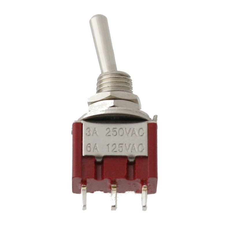
For today’s project, I thought it will be a good idea to look at the latching toggle switch to see if we can create a cheaper alternative which can be used for ON/OFF switch operations in devices in large scale production. One of the major factors behind the cost of the latching toggle switch is that they are mechanical in nature, thus for our solution, we will ensure we don’t turn the same part by creating a soft latching switch circuitry but we will use a push-button instead.
Design Requirements
As with any design, we will start out by outlining the requirements for our Soft Latching Switch. All of the requirements are geared towards ensuring the cost is kept low and performance is either greater or of the same quality with the mechanical latching toggle switch. The requirements are:
- Standalone; The circuitry should be independent of the system in which it is to be deployed.
- Minimal Parts; It should use very little components to keep the size small and cost as low as possible.
- Basic Parts Only; We won’t be using any special/dedicated modules
- No current drawn when Off
- Cheaper than the mechanical latching toggle switch.
Designing the Switch
For today’s design, we will draw inspiration from a design by David Jones. The switch circuitry (shown in the schematics below) is made up of two transistors which could either be PNP or NPN. The transistors work hand in hand such that the flow of base current to turn “ON” one of the transistors turns ON the other transistor. To explain better, consider the schematics below.
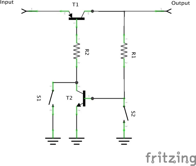
When the circuit is initially powered up, a chicken and egg kind of situation will be experienced as the transistor T2 will be off because there is no base current flowing through T1 (T1 is off) since the switch S1 has not been pressed. When the “on” Switch(S1) is pressed, current flows through the base of transistor T1, turning “on” the transistor and allowing the flow of current IC1 which then becomes a base current for transistor T2 (IB2). Both transistors are now “on”, thus the output is turned “on”. Because transistor T2 is connected in parallel to S1 it ensures the circuit stays on even when S1 bounces off, thus the system remains in its “on” state.
To turn the system off, the second momentary switch S2 needs to be pressed. S2 grounds the base of transistor T2 effectively turning the transistor off. This, in turn, breaks off the flow of the base current from transistor T1 to ground, turning off the transistor and effectively turning off the whole system.
While this circuit works and looks really simple, it doesn’t quite meet the requirements for our design as it requires 2x momentary switches instead of one, We want something similar to the Mechanical switch in operation, thus, there is a need for us to re-design this and remove the second switch. To do this, a few more components were introduced to arrive at the schematics below.
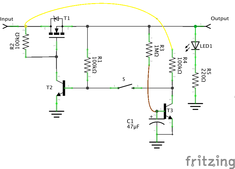
We start the redesign by changing transistor T1 from a PNP BJT in the previous circuit to a N-channel FET transistor. While the BJTs can do the job, FETs have better response and are more suitable for use in switching applications. The gate of the FET is tied to the input via resistor R2 to ensure it is not floating and the system stays off when switched off.
The second change is replacing the location of the switch and altering the design so switching is achieved using a single switch. This is done by the addition of transistor T3 to the circuit.
T3 is connected in such a way that when the switch is pressed for the first time, current (through the yellow wire) flows from the input to the base of transistor T2 through the switch(S), turning “on” T2 and creating a conduction path for the gate of T1, effectively turning “on” the system. Current is continuously supplied to the base of T2 through the resistor R1 after the switch is pressed.
The process of turning on the system also gets it ready to be turned off the next time the switch is pressed. As soon as the system is turned “on”, current is supplied to the base of Transistor T3 via resistor R3, turning “on” the transistor which shorts the current from the input (yellow wire) straight to ground. Thus, the next time the switch is pressed, the base of transistor T2 is grounded via the switch, turning “off” T2 which also turns “off” T1, effectively turning off the entire circuit. Because of the speed at which analog circuits responds and the possible slow speed at which the switch will be pressed by a user, a capacitor was used to allow the user enough time on each button press and to also serve as a debouncing mechanism for the switch. A LED is attached at the output to provide visual on/off feedback to the users.
Required Components
With the design ready we can now select the required components for it. While the values of resistors could be varied, it is important the values are sufficiently selected so current draw is enough and are symmetrical to keep the system balanced.
Based on the design, the following components are required;
- IRF9110n x1
- 2n3904 x2
- 100k Resistor x
- Resistor x 1
- 0ohms Resistor (1)
- 47uF Capacitor
- Led
- Jumper Wires
- Momentary Pushbutton (1)
For the transistors, I believe you can use any NPN BJT transistor with similar characteristics to the 2n3904 and for the N-Channel FET, the IRF9110 can be replaced with any other similar transistor, just ensure the Vgs of the transistor is compatible with the operating voltage.
Demo
With the design done, its time to test things out. Connect the components as shown in the main schematics. You should see the LED go on and off in line with the switch press.
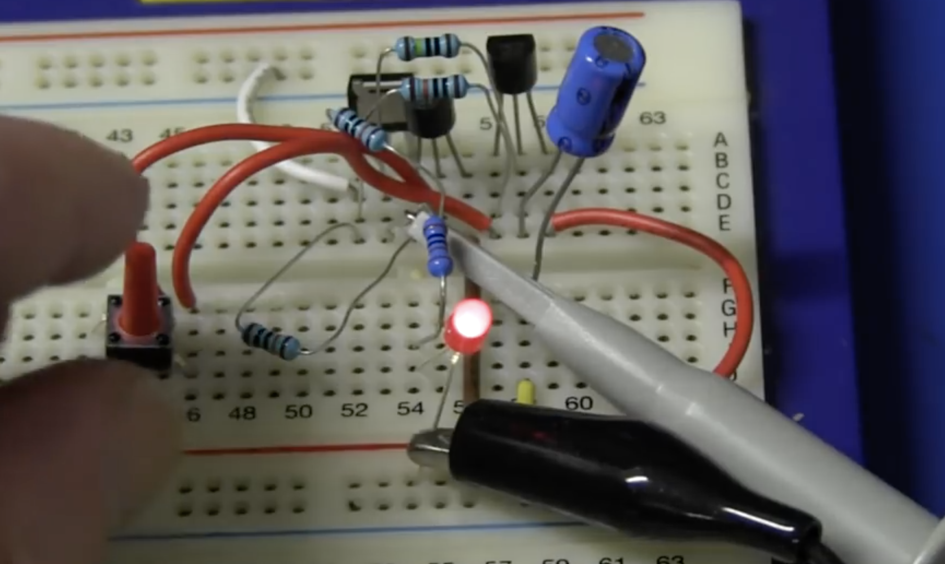
That’s it, this could easily replace mechanical latching toggle switch in your project. Try experimenting with the resistor and capacitor values to observe performance under different conditions.
Feel free to reach out to me via the comment section with questions or general comments on the project.


.png)


thank you for thise article …but i thinkthat T1 mosfet is P-Channel not as described in the explain!
and is very good when you can present other circuit with N-Channel
Thank you again
I am trying ti use the first diagram on this page for a project where I need separate off and on switches. The problem is there are no component values. I have a diagram I whipped up but no way to send it here. Can you please help with compoment values? markosjal AT gmail
The first diagram is just for reference. Please build the second one as it’s more stable.
100K resistors (like on second diagram) are just fine. BUT! As mixos mentioned this setup is unstable as it is. It would be perfectly stable, if components used were theoretically ideal, and there was no interference/noise from the background. But T1 and T2 form a positive feedback loop, and any imperfection turns it on (usually matter of seconds or less). But again, there is a remedy.
Bridge S2 with a R3 (also 100K; in other words, put it between base of T2 and ground), so it will keep weak connection to the ground, even when S2 is not pressed (closed). This will be enough to ground any noise buildup and leakage from T1. Now setup is stable in practice and guaranteed to start in off state. Addition of R3 has no measurable impact (in sub-micro-ampere range) on consumption of the circuit, which stays (without resistive load or load consumption deducted) at 88 microamperes (0.08mA) in on state, and zero (0) in off state in my test circuit (used BC557B for T1, BC547B for T1, and 100K 5% tolerance resistors; measured without load and with load of LED with 4,7K resistor).
Thank you for your great introduction!, I would like to have a question on Current direction at the switch. (I want to replace the momentary switch with a transistor, so that instead of using a button, I can use a trigger pulse from an output pin of micro-controller or a touch module (TTP223).
From your text and video, at the Switch:
+ 1st Press: current flow from right to left >> ON state
+ 2nd press: current flows from left to right >> OFF state
If it is a case, There is no way for me to use a transistor to replace the switch.
Please help to advice!