

Isolated Voltage-Measurement With ±1V Input and Differential Output with Integrated DC/DC Converter
- Rajkumar Sharma
- 39 Views
- easy
- Tested
- SKU: EL130694
- Quote Now

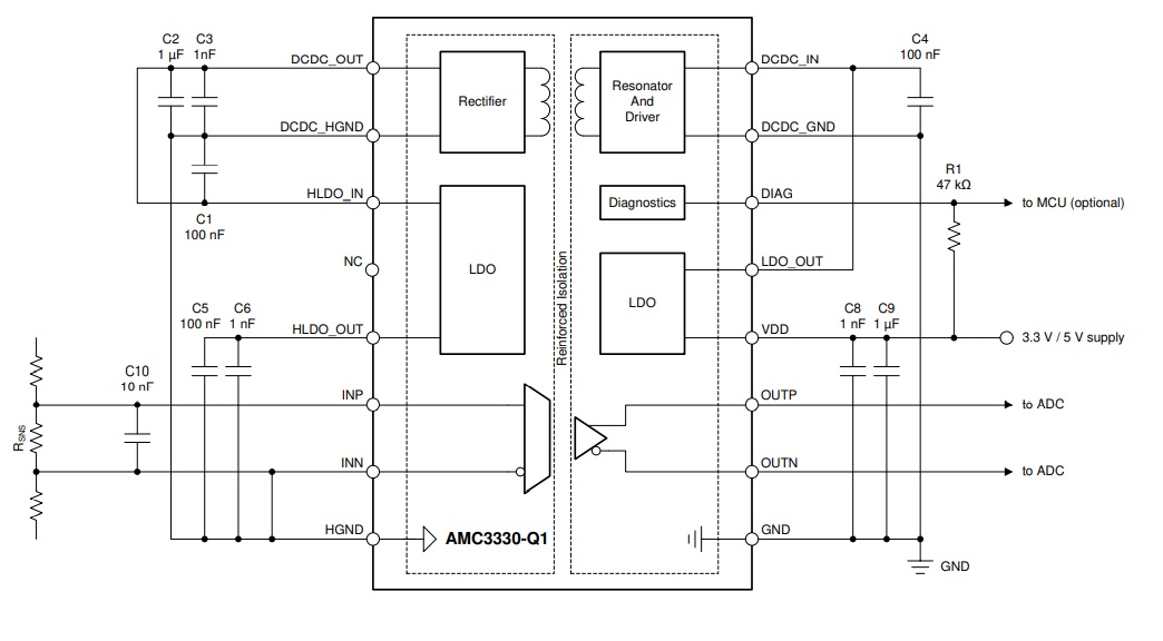
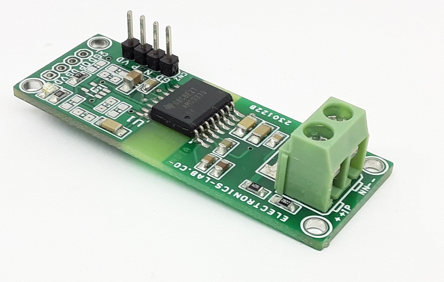
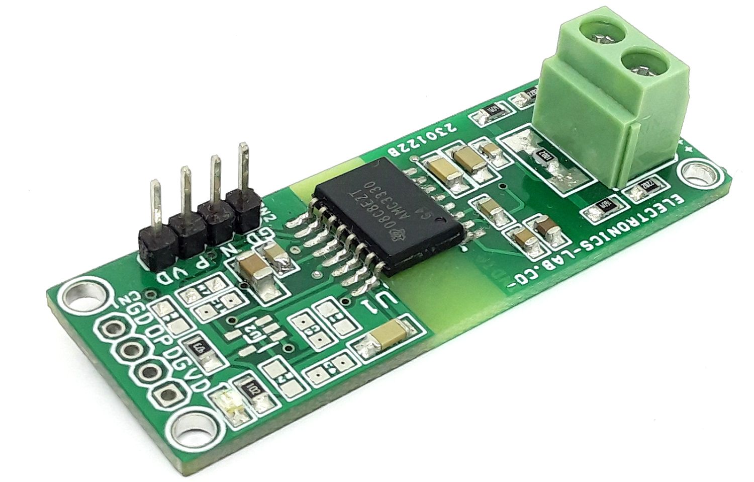
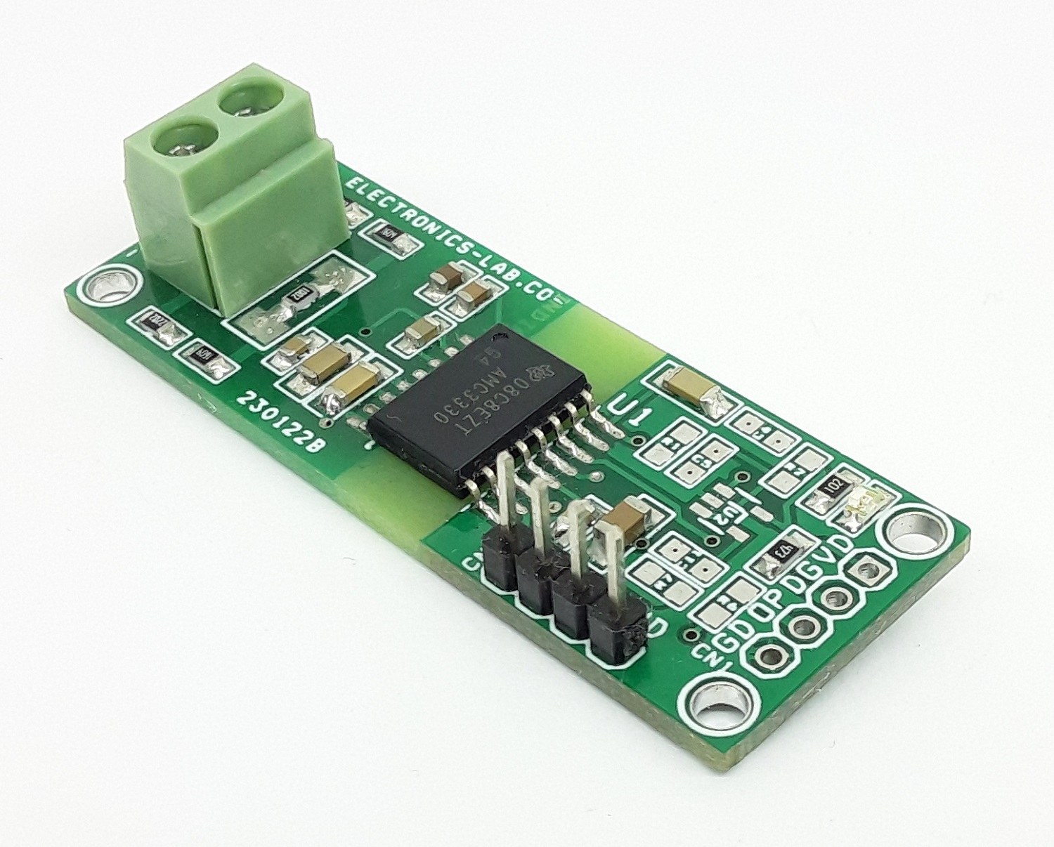
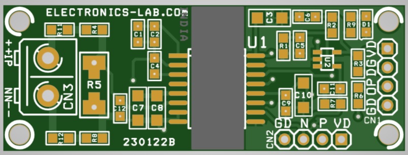
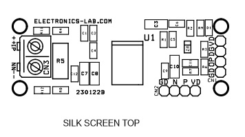
This project can be used in bidirectional high-voltage measurements. The output is fully isolated from the input side and can be used for applications such as high-voltage DC-DC converters, High-Voltage EV chargers, SMPS, 3 Phase motor drivers, inverters, etc. The board is built using the AMC3330 chip. The chip is a precision, isolated amplifier with a fully integrated, isolated DC/DC converter that allows single-supply operation from the low side of the device. The reinforced capacitive isolation barrier is certified according to VDE V 0884-11 and UL1577 and separates sections of the system that operate on different common-mode voltage levels and protect low-voltage domains from damage. The circuit senses high voltage in the range from -1V to 1V across resistor dividers R11, R4, R5, R8, and R12 and provides differential analog output Out-P and Out-N. The integrated isolated DC/DC converter allows the measurement of non-ground-referenced signals.
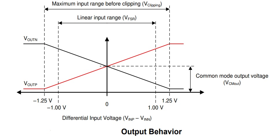
The board offers a differential analog output comprised of OUTP and OUTN pins. For differential input voltages (VINP – VINN) in the range from –1 V to 1 V, the device provides a linear response with a nominal gain of 2. For example, for a differential input voltage of 1 V, the differential output voltage (VOUTP – VOUTN) is 2 V. At zero input (INP shorted to INN), both pins output the same voltage, VCMout. For absolute differential input voltages greater than 1.0 V but less than 1.25 V, the differential output voltage continues to increase in magnitude but with reduced linearity performance.
Voltage Range and Divider Resistor Calculation
The project is optimized for 230V AC measurements, thus it can be modified for higher or lower voltage measurement range by altering the value of divider resistors R11, R4, R5, R8, R12. Current through resistor divider is 100uA, resulting in voltage drop on sense resistor R5 = 1V.
- For 230V-RMS Line Voltage (Peak Voltage 325V) R11=20K + R4=1.6M, R5 = 10K, R12 = 20K + R8=1.6M Tolerance 1%
- For 120V-RMS Line Voltage (Peak Voltage 170V) R11=25K + R4=820K, R5 = 10K, R12 = 25K + R8=820K Tolerance 1%
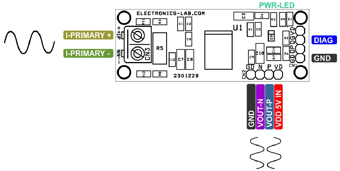
Connections and Other Important Details
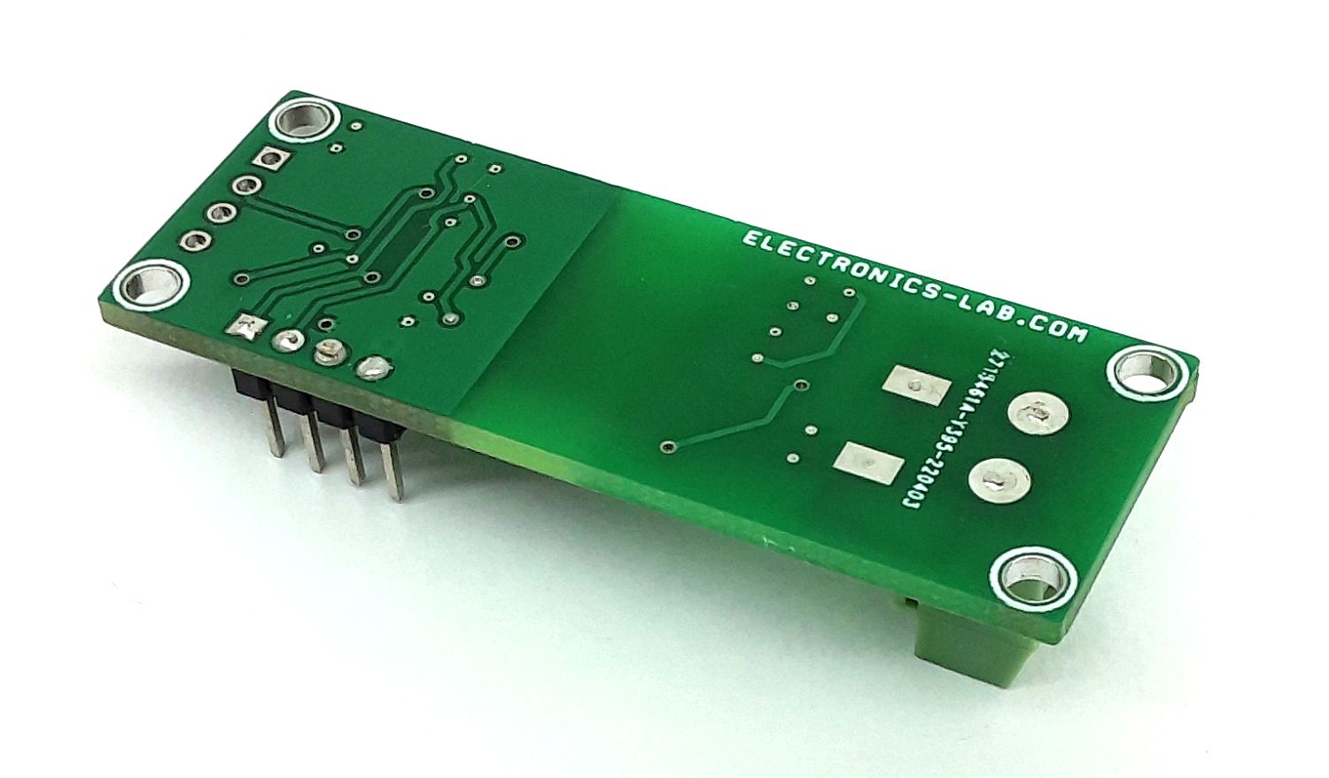
- CN1: Pin 1 = DIAG, PIN 2 = No Use, Pin 3 = Op, Pin 4 = GND
- CN2: Pin 1 = VDD 5V DC In, Pin 2 = Output-P, Pin 3 = Output-N, Pin 4 = GND
- CN3: Pin 1 = Primary Input +P, Pin 2 = Primary Input -N
- D1: Power LED
Features
- Power Supply Input 5V DC (Range 3.3V to 5V)
- ±1-V input voltage range optimized for voltage measurements with a high input impedance
- Fixed gain: 2.0
- 6000-VPK reinforced isolation
- Low DC errors: – Gain error: ±0.2% (max) – Gain drift: ±45 ppm/°C (max) – Offset error: ±0.3 mV (max) – Offset drift: ±4 µV/°C (max) – Nonlinearity: ±0.02% (max)
- Common Mode Output 1.44V (Voltage Output at zero 1.44V)
- Clipping Differential Output Voltage +/-2.49V (VOUT = (VOUTP – VOUTN); |VIN| = |VINP – VINN| > VClipping)
- Output Short-circuit Current 14mA
- PCB Dimensions 53.98 x 19.69mm
- 4 x 2.5 mm Mounting Holes
Diagnostic Output and Fail-Safe Behaviour
The open-drain DIAG pin can be monitored to confirm the device is operational, and that the output voltage is valid. During power-up, the DIAG pin is actively held low until the high-side supply is in regulation and the device operates properly. The DIAG pin is actively pulled low if:
- The low-side does not receive data from the high-side (for example, because of a loss of power on the high side). The amplifier outputs are driven to negative full-scale.
- The high-side DC/DC output voltage (DCDC_OUT) or the high-side LDO output voltage (HLDO_OUT) drop below their respective undervoltage detection thresholds VDCDCUV and VHLDOUV as specified in the Electrical Characteristics table. In this case, the low-side may still receive data from the high-side but the data may not be valid. The amplifier outputs are driven to negative full-scale. During normal operation, the DIAG pin is in a high-impedance state. Connect the DIAG pin to a pull-up supply through a resistor or leave open if not used.
Schematic

Parts List
| NO | QNTY | REF | DEC | MANUFACTURE | SUPPLIER | PART NO |
|---|---|---|---|---|---|---|
| 1 | 2 | CN1,CN2 | 4 PIN MALE HEADER PITCH 2.54MM | WURTH | DIGIKEY | 732-5317-ND |
| 2 | 1 | CN3 | 2 PIN SCREW TERMINAL PITCH 5.08MM | PHOENIX | DIGIKEY | 277-1247-ND |
| 3 | 1 | C1 | 1nF/16V CERAMIC SMD SIZE 0805 | YAGEO/MURATA | DIGIKEY | |
| 4 | 1 | C2 | 1uF/25V CERAMIC SMD SIZE 0805 | YAGEO/MURATA | DIGIKEY | |
| 5 | 2 | C4,C9 | 0.1uF/50V CERAMIC SMD SIZE 0805 | YAGEO/MURATA | DIGIKEY | |
| 6 | 8 | R1,R2,C5,R6,C6,R7,R10,C11 | DNP | DO NOT INSTALL | ||
| 7 | 2 | C3,C7 | 0.1uF/50V CERAMIC SMD SIZE 1206 | YAGEO/MURATA | DIGIKEY | |
| 8 | 1 | C8 | 1nF/25V CERAMIC SMD SIZE 1206 | YAGEO/MURATA | DIGIKEY | |
| 9 | 1 | C10 | 10uF/25V SMD SIZE 1206 | YAGEO/MURATA | DIGIKEY | |
| 10 | 1 | C12 | 10nF/50V SMD SIZE 0805 | YAGEO/MURATA | DIGIKEY | |
| 11 | 1 | D1 | LED RED SMD SIZE 0805 | OSRAM | DIGIKEY | 475-1278-1-ND |
| 12 | 1 | R3 | 47K 5% SMD SIZE 0805 | YAGEO/MURATA | DIGIKEY | |
| 13 | 2 | R4,R8 | 1.6M 1% SMD SIZE 0805 | YAGEO/MURATA | DIGIKEY | |
| 14 | 1 | R5 | 10K 1% SMD SIZE 1206 OR 2512 | YAGEO/MURATA | DIGIKEY | |
| 15 | 1 | R9 | 1K 5% SMD SIZE 0805 | YAGEO/MURATA | DIGIKEY | |
| 16 | 2 | R11,R12 | 20K 1% SMD SIZE 0805 | YAGEO/MURATA | DIGIKEY | |
| 17 | 1 | U1 | AMC3330 | TI | DIGIKEY | 296-AMC3330QDWERQ1TR-ND |
| 18 | 1 | U2 | TLV6001IDBVR | TI | DO NOT INSTALL |
Connections
Output
Application Example


Gerber View
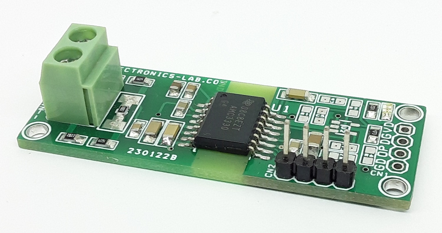
Photos

Video
AMC3330 Datasheet


PCB

.png)


")

