Search the Community
Showing results for tags 'mosfet'.
-
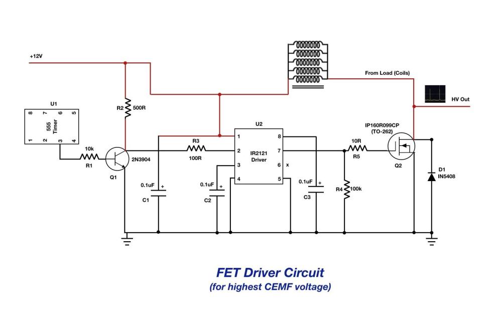
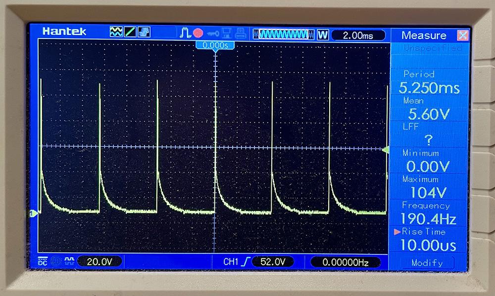
I have built a circuit for which the aim is to produce high voltage back EMF spikes from the Drain of a MOSFET so I can investigate some of the properties of these voltage transients. What I have built is shown in the attached circuit where I am using an IR2121 driver chip to encourage shorter shut off times and so produce higher voltage spikes. Going from a circuit that didn't use a driver chip to one that does has increased the voltage from about 800V to 1,040V as shown in the scope image using a 10:1 voltage divider. I have read that there are ways to further reduce the FET shut off time but as electronics is not my main discipline I find them rather confusing. For example, reducing the Gate bias resistor (R5) further (to 5R?) or putting a small capacitor (1nF?) across R5 and keeping the PCB track resistance from R5 to the Gate of Q2 as short as possible. I would appreciate any suggestions. Thanks
-
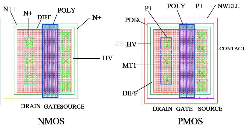
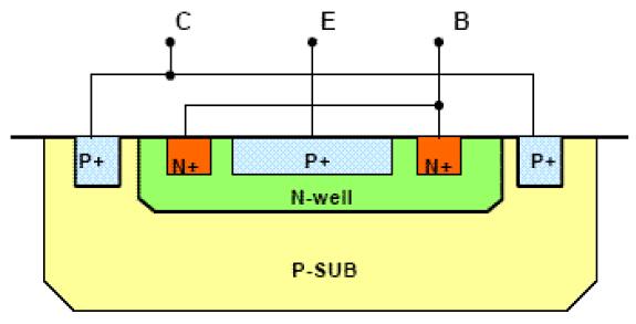
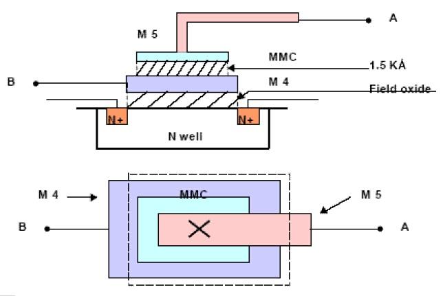
PCB Layout Tutorial: For High-Quality PCB Design http://www.apogeeweb.net/article/89.html Asymmetric source/drain MOS transistor LPNP MMC
-
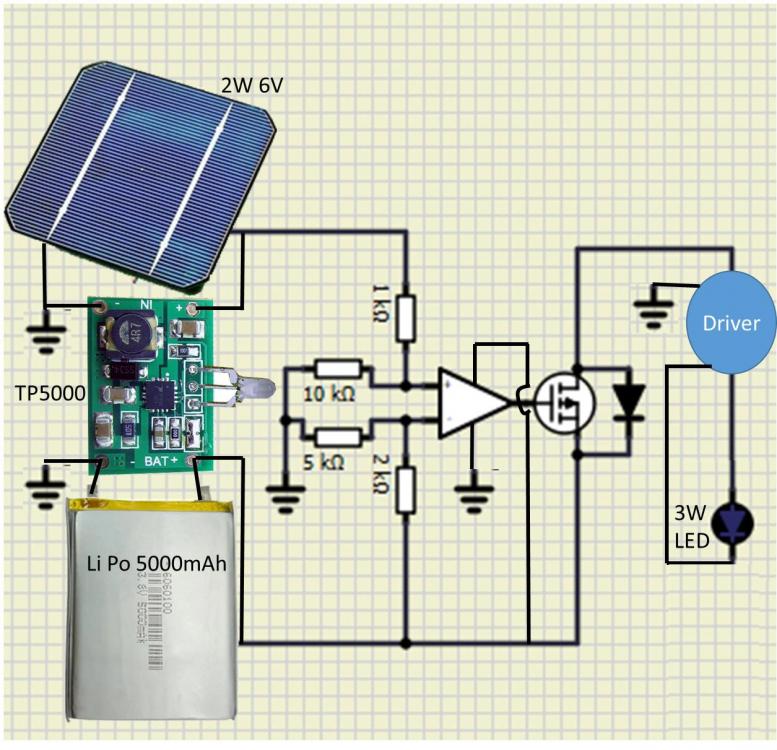
Hello. I would like to make a garden solar lamp that automatically turn on when the sun goes down. I tryed first with a transistor s9013 npn (seen on youtube), but it restricted the current, i suspect because of the internal resistance of the transistor. I decided to try the use of an Op amp as comparator, with a low internal resistance P channel Mosfet. I don't have much experience with these components, and the best way of learning is trying right? So see below my circuit. My problem is that it seem to work fine when the battery is full but the solar charging doesn't seem to be very efficient (the charge light does turn ON) and the battery looses it's charge fast, leading to a weired blinking LED. would anyone see a problem with my circuit explaining that? thank you very much for your help Best Damien


